|
|
|
|
|
|
| TDK developed and launched a high-performance FOUP model compatible with next-generation 450 mm wafers and a new model for 300 mm wafers that offers enhanced cost competitiveness |
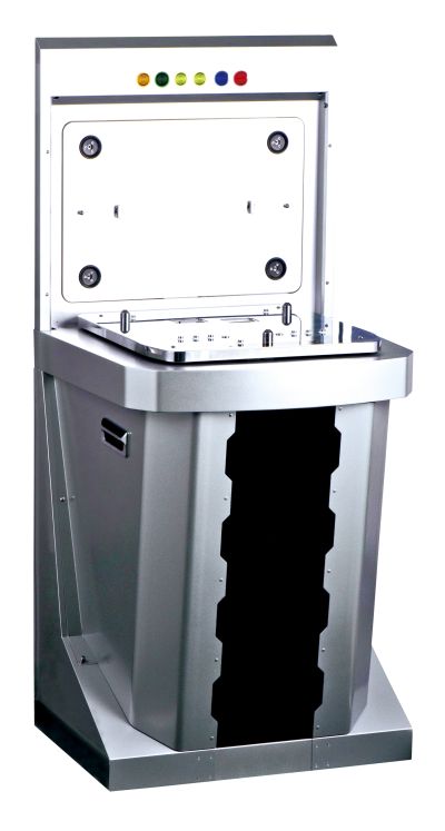
TOKYO, July 3, 2012 - (ACN Newswire) - TDK Corporation developed two new FOUP* load port models (the TAS450 Type A2 and the TAS300 Type J1) for a semiconductor production equipment. Sales of both models will begin in July 2012.
 | | TDK: New FOUP Load Port Models Launched |
An environment with a high degree of cleanliness is essential for state-of-the-art semiconductor device manufacturing processes, but this requires massive capital investment for large-scale air cleaning and other equipment. To control such capital investment, in recent years, automated transport systems that deliver semiconductor substrates (wafers) to completely sealed pods (FOUP) and shift the wafers between semiconductor production equipment have become the mainstream production method.
1. TAS450 Type A2
New model supports next-generation 450 mm wafers and controls particles at the industry's highest levels.
Main features:
This product is the first state-of-the-art transport system for semiconductor production that can accommodate the large-diameter 450 mm silicon wafers that are expected to be a next-generation technology in the semiconductor industry.
Key features of this product are an innovation applied to the opening and closing door that prevents particles from entering the semiconductor production equipment from outside during wafer input and output and prevention of the generation of particles from the load port itself.
2. TAS300 Type J1
New model achieves lighter weight and higher speed in the industry's highest level and seeks enhanced cost competitiveness.
Main features:
This product is a wafer transport system for 300 mm diameter wafers, which are currently used in manufacturing in the semiconductor industry, and was developed to provide higher cost competitiveness. The TAS300 Type J1 is the successor model to the Type H1 series introduced in 2009, and the overall weight of the load port has been reduced by half. In addition, door opening and closing for wafer input and output is approximately 40% faster than the H1 series. Like the TAS450 Type A2, an innovative door is used to prevent the generation and introduction of particles.
Glossary
- FOUP: A semiconductor wafer delivery pod standardized by SEMI, an industry organization for semiconductor production equipment makers.
Main applications
- Automated transport of silicon wafers between semiconductor production equipment.
You can download this text and associated images from www.global.tdk.com/news_center/press/aah40500.htm
Contact:
Japan,
Mr. Yoichi OSUGA,
TDK Corporation
+813 5201-7102, pr@jp.tdk.com

ASEAN,
Ms. Tomoko KAMEDA,
TDK Singapore (Pte) Ltd.
+65 6273 5022, asean.inquiry@sg.tdk.com

Greater China,
Ms. Clover XU,
TDK China Co., Ltd.
+86 21 61962307, pr@cn.tdk.com

Europe,
Mr. Frank TRAMPNAU,
TDK Electronics Europe GmbH
+49 211 9077 127, trampnau@eu.tdk.com

America,
Ms. Sara M. REYNOSO,
TDK Corporation of America
+1-972-409-4519, sreynoso@tdktca.com
Topic: New Product
Source: TDK Corporation
Sectors: Electronics, Daily Finance, Consumer Electronics
https://www.acnnewswire.com
From the Asia Corporate News Network
Copyright © 2026 ACN Newswire. All rights reserved. A division of Asia Corporate News Network.
|
|
|